Description
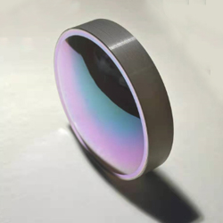
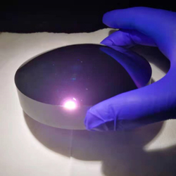
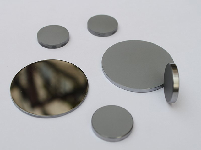
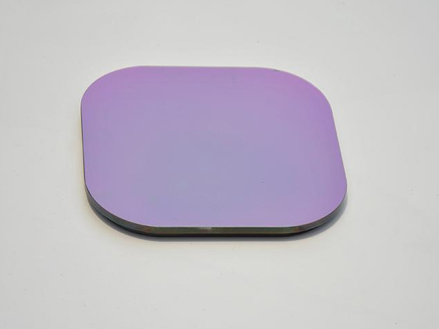
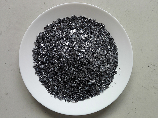
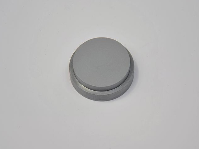
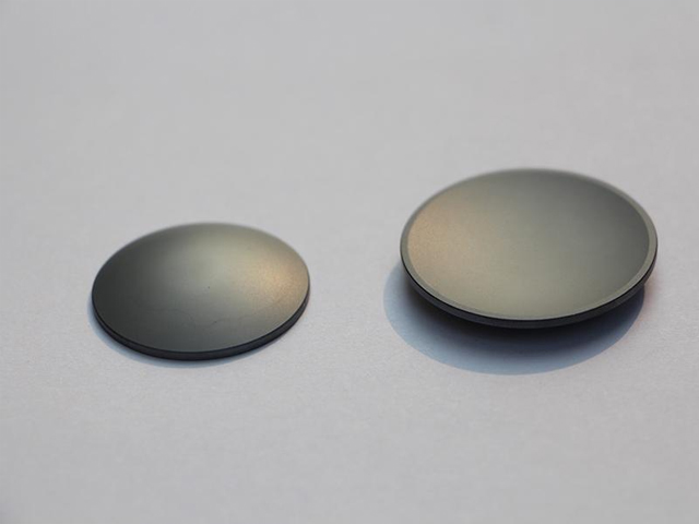
 Silicon polished sections are widely used in various fields of semiconductors. We have the ability to process 2-8 inch semiconductor monocrystalline silicon wafers, The quality of our products is checked at all levels, in the hope of providing customers with the highest quality products.
| Name | Silicon wafer |
| Growth Pattern | CZ or FZ |
| Type | P or N |
| Orientation | <100>or<111> |
| Diameter | 2-8 inch |
| Tolerance | ±5mm |
| Thickness | 180-2000μm |
| Tolerance | ±10μm |
| Dislocation Density(pcs/C㎡) | None |
| Resistivity | 0.001-10000 Ω.cm |
| Purity | 6N-9N |
| PARAMETER | UNIT | KORVXQ2B |
| GRADE | Prime | Prime |
| GROW METHOD | CZ | CZ |
| TYPE | P | |
| DOPANT | Boron | |
| XTAL ORIENTATION | DEGREES | 1-0-0 |
| RESISTIVITY CTR | W·CM | 10.0-20.0 |
| RRG 1 CTR-1/2R MAX | ﹪ | / |
| RRG 2 C-6mm MAX | ﹪ | 8.0 |
| SLICE ORIENTATION | DEGREES | 1-0-0±0.5° |
| OXYGEN CTR | NEW PPMA | 13.0-19.0 |
| ORG MAX | ﹪ | / |
| PRIMARY FLAT LOCATION | DEGREES | 1-1-0±0.5° |
| PRIMARY FLAT LENGTH | MM | 32.5±2.5 |
| SECONDARY FLAT LOCATION | DEGREES | N/A |
| SECONDARY FLAT LENGTH | MM | / |
| CARBON CTR MAX | PPMA | 1.0 |
| TTV MAX | MICRONS | 15.0 |
| BOW MAX | MICRONS | 40.0 |
| WARP MAX | MICRONS | 40.0 |
| EDGE CONTOUR | SEMI STD. | |
| FS PARTICLE | LIGHT | / |
| SIZE MAX | MICRONS | 0.5 |
| MAX | #/SL | 10.0 |
| DISLOCATION | #/Sq c㎡ | 100.0 |
| OISF MAX | #/Sq c㎡ | 100.0 |
| LASER MARK | N/A | |
| GLOBAL TIR MAX | MICRONS | 5.0 |
| SITE TIR MAX | MICRONS | / |
| SLICE BACK | Etched | |
| CUSTOMER PART NO | 4-thk1000-ssp | |
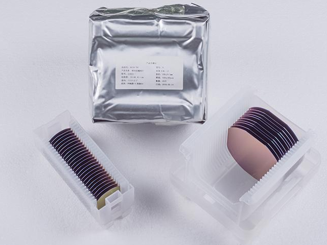
| PACKAGE | standard packaging | UPACK A 25片/box |
| REMARKS | Other unlisted parameters are executed according to SEMI standards | |

